Startseite Produktep type silicon substrate Online-Hersteller
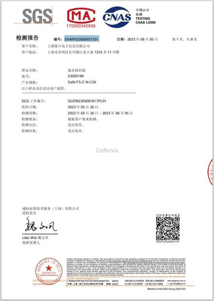
Bescheinigung
CHINA Shanghai GaNova Electronic Information Co., Ltd. zertifizierungen
Ich bin online Chat Jetzt

p type silicon substrate online manufacture

(81)
kaufen JDCD07-001-002 5-Zoll-SOI-Epitaxialwafer für die MEMS-Verarbeitung Online Hersteller

JDCD07-001-002 5-Zoll-SOI-Epitaxialwafer für die MEMS-Verarbeitung

5-inch SOI epitaxial wafer for MEMS processing Overview Silicon Wafers (Si Wafer) are thin slices of highly pure crystallized Silicon. Silicon wafers act as a substrate for microelectronic devices and are ... Lesen Sie weiter
2025-04-27 11:43:50
kaufen 0.015Ω•cm-0.025Ω•Epitaxial- Oblaten-C-Gesichts-optischer polnischer Si-Gesicht CMP cm sic Online Hersteller

0.015Ω•cm-0.025Ω•Epitaxial- Oblaten-C-Gesichts-optischer polnischer Si-Gesicht CMP cm sic

0.015Ω•cm—0.025Ω•cm SiC Epitaxial Wafer C-Face:Optical Polish,Si-Face CMP Overview A SiC wafer is a semiconductor material made of silicon. A silicon carbide wafer is a crystalline material that is made by ... Lesen Sie weiter
2024-10-29 11:49:58
kaufen JDCD07-001-003 6 Zoll SOI Epitaxial Wafer For MEMS Verarbeitung Online Hersteller

JDCD07-001-003 6 Zoll SOI Epitaxial Wafer For MEMS Verarbeitung

6-inch SOI epitaxial wafer for MEMS processing Overview In electronics, Silicon wafers (also known as substrates) are thin slices of highly pure crystalline Silicon (c-Si), used in the production of integrated ... Lesen Sie weiter
2025-04-04 22:42:31
kaufen JDCD07-001-004 7-Zoll-SOI-Epitaxialwafer für die MEMS-Verarbeitung Online Hersteller

JDCD07-001-004 7-Zoll-SOI-Epitaxialwafer für die MEMS-Verarbeitung

7-inch SOI epitaxial wafer for MEMS processing Overview A silicon wafer is a material essential for manufacturing semiconductors, which are found in all kinds of electronic devices that enrich our lives. Few of ... Lesen Sie weiter
2025-04-27 11:43:50
kaufen Zoll GaN Epi Wafer Dimensions der Stärke-370um 430um 2 50mm Online Hersteller

Zoll GaN Epi Wafer Dimensions der Stärke-370um 430um 2 50mm

Thickness 400 ± 30 μm 2-Inch Free-Standing N-GaN Substrates Dimensions 50.0 ±0.3 mm 2inch C-face Si-doped n-type free-standing GaN single crystal substrate Resistivity < 0.05 Ω·cm Power device/laser wafer ... Lesen Sie weiter
2024-10-29 11:49:57
kaufen JDCD07-001-001 4-Zoll-SOI-Epitaxialwafer für die MEMS-Verarbeitung Online Hersteller

JDCD07-001-001 4-Zoll-SOI-Epitaxialwafer für die MEMS-Verarbeitung

4-Inch SOI Epitaxial Wafer For MEMS Processing Overview Although silicon crystals may look metallic, they are not entirely metals. Due to the "free electrons" that move easily between atoms, metals are good ... Lesen Sie weiter
2025-04-27 11:43:50
kaufen JDZJ01-001-004 SiC-Ingot-Kristall 6&quot; P-Klasse Online Hersteller

JDZJ01-001-004 SiC-Ingot-Kristall 6" P-Klasse

SiC ingot crystal 6" Pgrade Silicon carbide, exceedingly hard, synthetically produced crystalline compound of silicon and carbon. Its chemical formula is SiC. Since the late 19th century silicon carbide has ... Lesen Sie weiter
2025-04-04 22:42:33
kaufen GaN-Epitaxialwafer ist für die Produktion von Hochspannungs-Hochfrequenzchips unerlässlich Online Hersteller

GaN-Epitaxialwafer ist für die Produktion von Hochspannungs-Hochfrequenzchips unerlässlich

Description: Epiaxial wafers refer to products formed by growing a new single crystal layer on a single crystal substrate. Epiaxial wafers determine about 70% of the performance of devices and are important raw ... Lesen Sie weiter
2024-12-06 17:47:04
kaufen Halbleiterbauelemente 8-Zoll- Wafer 775um 725um 675um Online Hersteller

Halbleiterbauelemente 8-Zoll- Wafer 775um 725um 675um

2-Inch Silicon Wafer Thickness Tolerance Standard ± 25μm,Maximum Capabilities ± 5μm 2-Inch Silicon Wafer MEMS Devices, Integrated Circuits,Dedicated Substrates For Discrete Devices Overview Nearly all the ... Lesen Sie weiter
2022-09-27 16:50:19
kaufen JDWY01-001-002 2 Zoll dicker Film (1,2)Um AIN auf Saphirwafer DSP XRD FWHM Von(002)≤80arcsec(102) ≤650arcsec Online Hersteller

JDWY01-001-002 2 Zoll dicker Film (1,2)Um AIN auf Saphirwafer DSP XRD FWHM Von(002)≤80arcsec(102) ≤650arcsec

2 inch thick film (1,2)um AIN on sapphire wafer,DSP,XRD FWHM of(002)≤80arcsec(102) ≤650arcsec UV disinfection, LED chip A thin film of aluminum nitride is a form of semiconductor material. It is highly ... Lesen Sie weiter
2025-04-27 11:43:50
Page 8 of 9|< 1 2 3 4 5 6 7 8 9 >|